SNES Controller PCB Instructions (Through-Hole Edition)
1. Preparation
Attention
This document is for the Through-hole edition PCB. If you're looking for assembly instructions for the Lighted SOCD Edition PCB using SMD parts, those instructions are right here
Note
I put some Amazon Affiliate links in this section. I get a miniscule commission (at no cost to you) if you buy stuff with these links, but every little bit helps right?
Required Tools
You need some basic soldering equipment for this:
- Soldering Iron and Solder (I use this one)
- De-Soldering Braid to clean up solder bridges - accidental or intentional (I use this stuff)
- Flux (like this stuff)
Optional Tools
These tools are mostly only needed if you're going to replace the connector on the end of the SNES controller cable that plugs into the PCB.
- Wire cutting tool
- Wire stripping tool
- Dupont terminal crimping tool (like this one)
Donor Components
If you are repairing a broken controller, you should harvest the following components from the original unit:
- Shell, screws, d-pad, buttons, shoulder button pivot pins, and membranes.
- Alternative: Transparent d-pad, buttons, and membranes to take advantage of the optional LEDs.
- Shoulder button daughter boards and wires.
- Alternative: Fabricate new shoulder button daughter boards.
- Wire-to-board header that mates with the original connector on the controller cable.
- Alternative: Use a Molex Mini-SPOX™ connector as documented in Wire-to-Board Header/Option 2
Required Knowledge
I'm not going to try and teach you any of these things in these instructions, so best come prepared. You should already know:
- How to use all of the tools on the Required and Optional lists.
- How to solder and de-solder through-hole components.
- How to handle static-sensitive parts.
- Basic electronic safety precautions.
Before You Begin
- Carefully sort and identify your parts.
- Make sure you understand how to identify proper polarity for all components. Refer to the manufacturer datasheet if you have any doubts.
- Take a minute to familiarize yourself with the PCB layout and conventions used in the silkscreen markings:
- Where applicable, PIN 1 is identified with a square solder via.
- Additionally, the IC orientation is indicated by the silkskreen - match the divot in the top of the IC up with the divot in the silkscreen.
- The proper orientation of the wire-to-board header is indicated with a line around the outside and, in the case of the Nintendo OEM footprint, keyed with peg holes.
2. Basic Controller Function
Applicable Board Revisions: ALL
This section populates the components required for this SNES controller PCB to be a SNES controller.
Required BoM Components
These are really common parts available from lots of places. The table below includes Amazon (affiliate) and Digikey links.
| Ref | Mfg. Part # | Quantity | Description |
|---|---|---|---|
| U1, U2 | CD4021BE (Amazon) CD4021BE (Digikey) |
2 | CMOS 8-Stage Static Shift Register, 16-PDIP |
| R1, R2 | A103J (Amazon) 4309R-101-104LF (Digikey) |
2 | Bussed 8 Element Resistor array, 10Kohms 50V 2%, 9-SIP |
| C1 | Esx-9Xh31akJgWX-5,100NF (Amazon) K104K15X7RF5TL2 (Digikey) |
1 | Ceramic Disc Capacitor, 0.1uF 50V, through-hole |
Note
With the exception of the CD4021B, the above part numbers should be treated as example only. If a specific part number happens to be discontinued, a suitable replacement is fairly easy to source just by searching for the required value and package type.
Assembly Steps - Part 1
Note
All components should be soldered on the back side (the side opposite the button contacts) of the PCB. The shift registors and resistor arrays are each 5mm tall when fully seated, which makes them about 1.5mm too tall for the front size of the board.
- Solder CD4021B shift registers at U1 and U2. Pin 1 is marked by a .
- Solder 10K resistor arrays at R1 and R2. Pin 1 is marked by a square solder via.
- Solder 0.1uf ceramic capacitor (marking:
104) at C1.
Trimming Component Leads
Placement of the resitor arrays at R1 and R2 is one of the compromises I had to make in this design variant. Their current placement was about the best I could manage without significantly altering the shape and size of the PCB itself, but their position makes it incredibly important that the legs be trimmed as flush as possible to the PCB to avoid colliding with the PCB supports in the front face of the controller housing.
3. Wire-to-Board Header
I saved this for last because it contains two options:
- Salvaged connector from a Nintendo SNES controller OR
- New Molex Mini-SPOX connector.
Which of these you use is entirely up to you, but using the original connector from a SNES controller is generally preferred because it means you don't have to re-wire a controller cable.
Option 1 (RECOMMENDED)
Salvaged Nintendo Connector
This is the best option if you have a rev_4a or newer PCB and are not building something completely custom. There is no BoM for this, just de-solder the connector from the old SNES controller and solder it in the J2 footprint on the PCB.
Option 2
Molex Mini-SPOX
Warning
Be advised: special tools are required for this option.
Required BoM Components
| Ref | Mfg. Part # | Quantity | Description |
|---|---|---|---|
| J1 | 22-05-7055 |
1 | Molex Mini-SPOX 5-pin horizontal header |
| N/A | 50.37-5053 |
1 | Mini-SPOX 5-pin plug |
| N/A | 39-00-0160 |
5 | Mini-SPOX TERM 22-28G FEM |
Minimum Order Quantity
Most places require you to buy at least 100 of the crimp terminals for these connectors. They're usually very cheap and easy to mess up when criming, so having extras is not the worst thing in the world.
Assembly Steps
- Solder the Mini-SPOX header to the J1 footprint on the PCB.
-
Cut the old Ninendo connector off the BOARD-END of the controller cable.
Caution
I said BOARD-END! That's the end that plugs into the header on the controller PCB, NOT the end that plugs into the SNES control deck!
-
Strip about 2mm of insulation off of the wires and crimp Mini-SPOX terminals onto them.
- Orient a Mini-SPOX 5-pin plug as it would plug into the header. That's wire-side facing you and bumpy-side down.
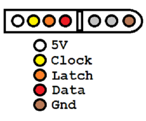
- Slot the terminals into the plug in this order (left-to-right):
- WHITE : +5V
- YELLOW : Clock
- ORANGE : Latch
- RED : Data
- BROWN : Ground
Info
If have any doubts about which wire goes where, I suggest you refer to this SNES controller pinout diagram and tone the pins out with a meter:
4. Final Assembly
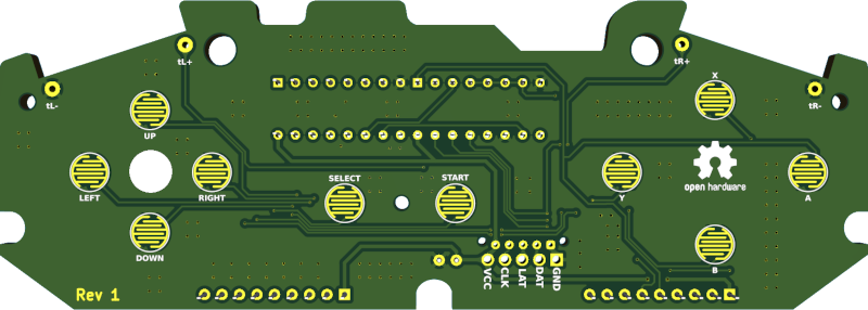
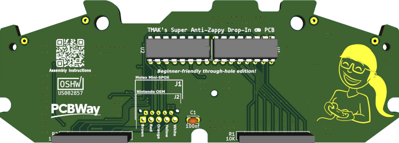
If you've made it this far, you should have a fully assembled board that resembles this:
Final assembly steps:
- Solder wires from each shoulder button daughter board to the tR+/tR- and tL+/tL- vias on the main controller PCB.
- Connect the controller cable to the header on the PCB.
- Reassemble your controller and test it to ensure everything is working as expected.
- I recommend using either the SNES Burn-In Test Cart or 240p Test Suite for this.
- Go play your Super Nintendo/Super Famicom!
5. Troubleshooting
Oh no! You've finished assembling your shiny new controller board but it doesn't work right! Here are some common symptoms and possible causes.
| Symptom | Have a look at... |
|---|---|
| Controller registers random/spazzy button inputs even when nothing is pressed. May affect some or all buttons. | Floating shift register parallel inputs due to poorly soldered resistor array(s). |
| No input at all registered from controller. | (1) Solder bridge between U2 pins 10 & 11. (2) Solder bridge between pins 1 & 2 or 4 & 5 on the wire-to-board header (PCB side) (3) Dry solder joints on the wire-to-board header (PCB side). (4) Loose or damaged wires/pins in the wire-to-board connector (cable side). |